Yale Engineers develop breakthrough method for practical nanowire materials
One-dimensional topological nanomaterials - that is, extremely thin nanowires - hold great promise for quantum and electronic devices, but certain limitations have kept them from being put to practical use. Now a team of researchers have developed a method for creating these materials that’s quick and easy to scale up. The results are published in Matter.
“The topological material in nanowires conducts electricity on the surface and only on the surface,” said Jan Schroers, Robert Higgin Professor of Materials Science & Mechanical Engineering, who led the study. So if you have a macroscopic material, he points out, then only a few of the material’s atoms are doing the work. With extremely thin nanowires, though, you have a higher percentage of atoms conducting electricity, increasing the overall efficiency of the system.

The problem:
Making nanowires, though, is no easy trick. The conventional method for making nanowires involves adding atoms layer by layer. It’s extremely complicated, time-consuming, and requires great precision. It also makes it very difficult to scale up the manufacturing to allow the practical use of nanowires at the industry level.
The solution:
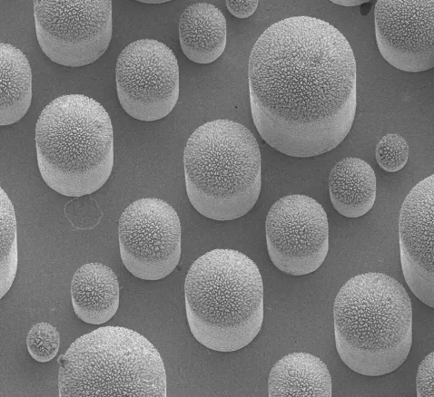
The method devised by the Schroers Lab, though, uses changes in pressure to guide the atoms where they need to go. Specifically, they press the material - at an elevated temperature, but not the melting point - against extremely small chambers, or nanocavities. The atoms then automatically move from a high-pressure environment to a low-pressure one into the nanocavity to form single-crystal nanowires.
“The way we made them, they’re almost self-organizing,” Yi-Xiang Yang, the graduate student leading the experimental aspect of this work said. “Each individual atom goes from the bulk material to the tip of the nanowire and then it just finds where the best energetic spot is. That creates these structures. And it is shockingly precise, and shockingly well-organized.”
In addition to being easier and expanding the number of potential materials that can be used for nanowires, this process is about 100 times faster than conventional methods.
Why it matters:
A practical means for manufacturing nanowires at a large scale could be a huge boon for industries and research fields specializing in quantum computing, optoelectronics and others. For instance, the unusual properties of nanowires make them ideal for transporting qubits, the unit of information in quantum computing. They could also be used to create lasers for photonic chips - speedier and more efficient than those in conventional electronics. And their size will help meet the demand for ever smaller electronics.
Going forward:
The Schroers Lab is collaborating with a research group in Taiwan. Using samples produced by the Schroers group, the Taiwan lab is now building devices with them. “The results are very encouraging,” Schroers said.
Bonus fact: The nanowires created by Schroers’s method are between 2.5 and 60 nanometers in diameter – up to 40,000 x thinner than the human hair.
More Details
Published Date
Aug 8, 2025


